Publisher's Synopsis
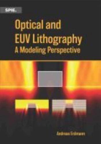
State-of-the-art semiconductor lithography combines the most advanced optical systems of our world with cleverly designed and highly optimized photochemical materials and processes to fabricate micro- and nanostructures that enable our modern information society. The precise fabrication and characterization of nanopatterns requires an in-depth understanding of all involved physical and chemical effects. This book supports such an understanding from a model-driven perspective, but without a heavy mathematical emphasis. The material for the book was compiled during many years of lecturing on optical lithography technology, physical effects, and modeling at the Friedrich-Alexander-University Erlangen-Nuremberg and in preparation for dedicated courses on special aspects of lithography. The book is intended to introduce interested students with backgrounds in physics, optics, computational engineering, mathematics, chemistry, material science, nanotechnology, and other areas to the fascinating field of lithographic techniques for nanofabrication. It should also help senior engineers and managers expand their knowledge of alternative methods and applications.
